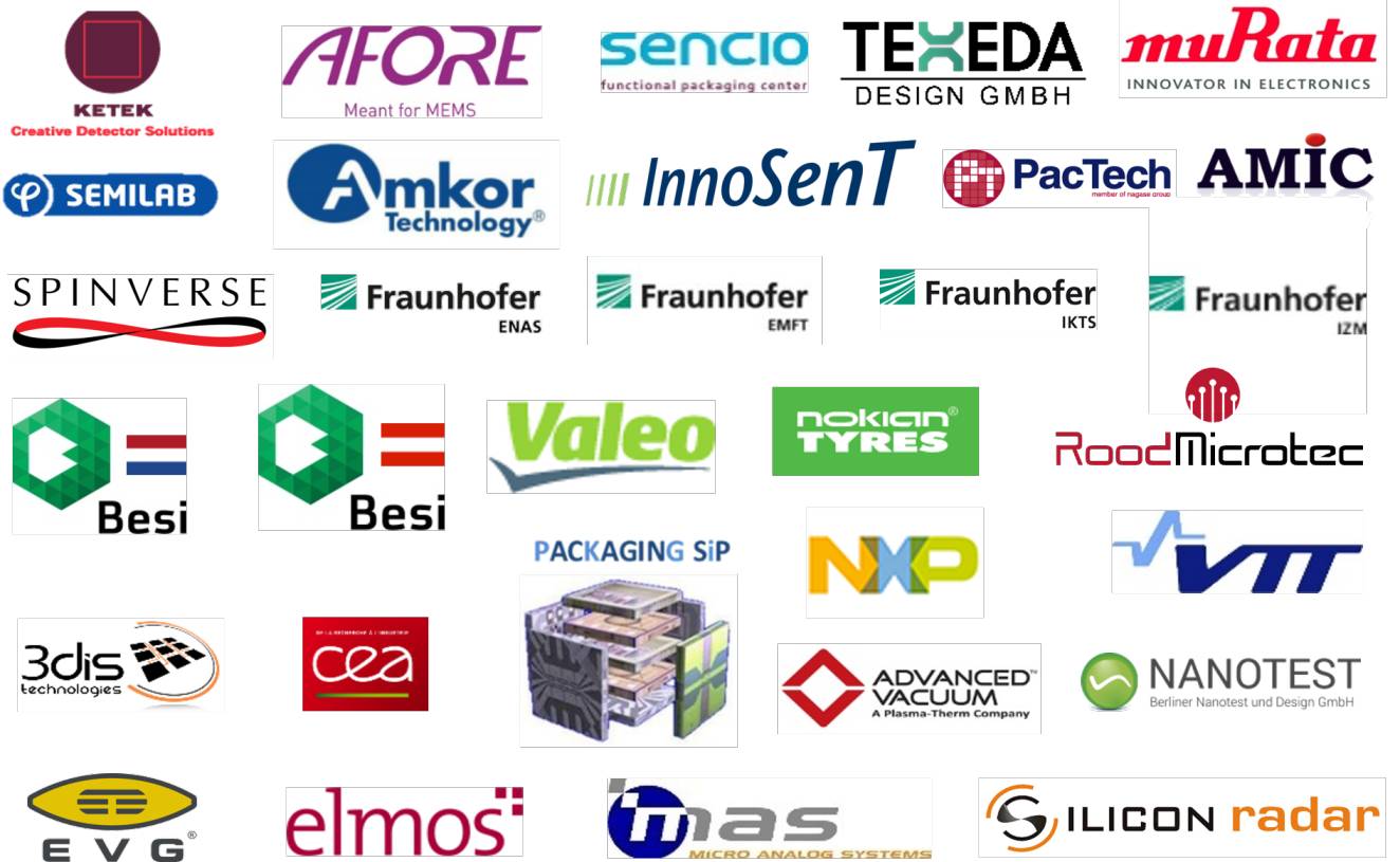
The EuroPAT-MASiP project with 28 partners from all over Europe was completed in August 2021, demonstrating a successful and significant overall outcome. The project, funded by the ECSEL JU and national funding agencies, aimed to reinforce the European semiconductor manufacturing position by focusing on the semiconductor and microelectromechanical systems (MEMS) packaging. The results of the project have an impact on the development of new packaging technologies, production and test equipment, as well as on innovative applications by European electronics, component and system manufacturers. Spinverse prepared the funding application and supported the project coordinator on the project’s day-to-day management, communications and dissemination.
Today, no industrial product, nor entertainment system is conceivable without extensive usage of electronic components and sensors. As these components get more complex and contain a heterogeneous variety of different elements, the role of electronics packaging becomes even more important. The demand and requirements from industry have always been one of the strongest technology drivers for advanced electronics packaging.
The main goals of the EuroPAT-MASiP project (European Packaging, Assembly and Test Pilot for Manufacturing of Advanced System-in-Package) were to support the European packaging ecosystem by developing key building blocks for future packaging needs: packaging related processes, equipment and materials, advanced packaging and integration technologies, packaging design and simulation and testing, metrology and failure analysis. The technologies were demonstrated in six product-like pilots and even real products.
The completed project demonstrates promising results
According to the official review report by the European Commission released in autumn 2021, the project achieved results with significant exploitation and impact potential.
One of the main results was the demonstration of the fan-out wafer level packaging (FO-WLP) process of electronic components packaging at an industrial scale. This method is also suitable for low-volume production or complex sensors, making it possible for innovative small and medium-sized enterprises (SMEs) to scale up production and reach the market easier — this is a major success of the EuroPAT-MASiP project.
Packaging processes, such as FO-WLP, were demonstrated in six industrial application pilots: 1) Integrated circuits for WLAN transceivers, 2) Silicon photomultipliers, 3) Car tyre sensors, 4) Automotive inertial sensors, 5) Autonomous guided vehicle radar sensors and 6) High-performance camera modules for automotive applications. The most exceptional results, related to virtual prototyping of System in Package (SiP) products, were developed in collaboration with the Finnish branch of the global MEMS sensor manufacturer Murata and the German research organisation Fraunhofer ENAS, who plan to continue the collaboration in the future. The application pilot developed by NXP France, for example, was also showing promising results.
Senior Project Manager Satu Ek managed the project from Spinverse side. She summarized: “We are delighted to see that our support to project coordination and dissemination and exploitation of the results was considered beneficial and helped the coordinator and the project consortium achieve visibility among the component manufacturing sector and the partners to focus on their technical work.”
![]()
The EuroPAT-MASiP project with 28 partners from all over Europe was partially funded by the Horizon 2020 ECSEL-IA with 7.2 M€.
More information: EuroPAT-MASiP website
Consortium: